Updated:2025-04-09
Silicon Carbide (SiC) MOSFETs are metal-oxide-semiconductor field-effect transistors fabricated using the wide-bandgap semiconductor material SiC. Compared with traditional silicon (Si) MOSFETs, they exhibit superior characteristics including higher breakdown voltage, lower on-resistance, faster switching speeds, and enhanced high-temperature/high-frequency performance.
Case Overview: Dynamic testing of SiC MOSFETs enables acquisition of critical parameters such as switching speed and switching losses, assisting engineers in optimizing chip design and packaging. However, the extremely fast switching characteristics of SiC MOSFETs impose stricter requirements on the parasitic parameters of measurement systems. Parasitic inductance and capacitance may compromise testing accuracy, necessitating optimization and control measures.
Test Case
Device Under Test (DUT): CREE C3M0075120K SiC MOSFET
Test Points: Drain-source voltage (Vds) and gate-source voltage (Vgs)
Test Challenges: Conventional passive probes and standard differential voltage probes exhibit excessive parasitic parameters. Due to the ultra-fast switching speeds of SiC MOSFETs (high dv/dt), probe parasitic inductance and capacitance can couple with the test circuit, causing significant oscillations or overshoot in the measured voltage signals. Additionally, parasitic capacitance may introduce displacement currents, superimposing spurious components onto the measured current signals and compromising overall measurement accuracy.

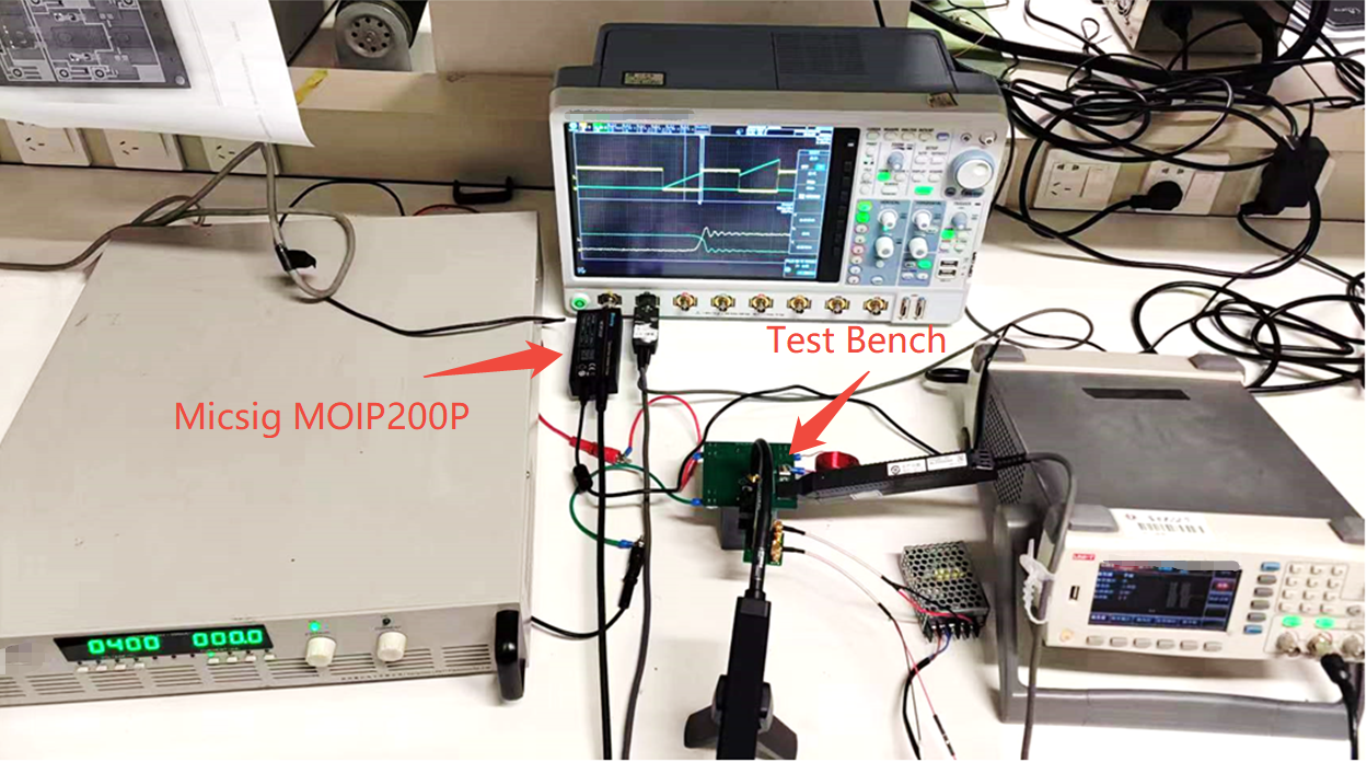
SiC MOSFET Dynamic Test Platform with Micsig MOIP200P SigOFiT Optical-fiber Isolated Probe
Test Evaluation
A dynamic test platform was established to evaluate the switching characteristics of SiC MOSFETs. The platform employed C3M0075120K SiC MOSFETs paired with C4D10120A freewheeling diodes. The switching process was controlled by gate driver UCC21520.
To ensure measurement accuracy:
Drain-source voltage (Vds) and gate-source voltage (Vgs) were measured using Micsig MOIP200P optically isolated probes, featuring:
o 200MHz bandwidth
o 180dB common-mode rejection ratio (CMRR)
o Ultra-low parasitic capacitance (1pF)
Drain-source current (Ids) was captured using Hioki 3276 clamp current probe (100MHz bandwidth)
Voltage and current probes were synchronized through time alignment calibration circuits
Waveform Sequence (top to bottom):
1.Gate-source voltage (Vgs)
2.Drain-source voltage (Vds)
3.Drain-source current (Ids)
Test Observations:
SiC MOSFETs demonstrated sub-20ns switching transitions
Observed waveform oscillations primarily originated from parasitic inductance in power loops (normal phenomenon)
EMI interference during high-speed switching was effectively mitigated by optical isolation technology
Advantages of Optically Isolated Probes:
1.High CMRR (180dB) ensures accurate signal capture in high-EMI environments
2.Ultra-low parasitic capacitance (1pF) minimizes displacement current errors
3.Fiber-optic transmission eliminates ground loop interference
4.Preserved waveform integrity enables precise switching loss calculations

Dynamic Test Results of SiC MOSFET Using Micsig MOIP200P SigOFiT Optical-fiber Isolated Probe
Client Feedback
The MOIP200P probes demonstrated:
· Effective suppression of high-frequency EMI via 180dB CMRR
· Undistorted Vgs and Vds waveforms matching simulation results
· Reliable data foundation for switching loss analysis
Technical Breakthroughs vs Traditional Methods
Traditional Measurement Limitations:
1.Parasitic Interference
High parasitic capacitance (10-50pF) → displacement current artifacts
Excessive inductance → voltage oscillations masking true switching waveforms
2.EMI Susceptibility
Low CMRR (<60dB) → waveform distortion from high dv/dt
Ground loop interference → potential device failure risks
SigOFiT Optical-fiber Isolated Probe Advantages:
1.Precision Measurement Capability
1pF parasitic capacitance reduces current measurement error by 10-50×
180dB CMRR provides 1000× EMI suppression improvement
2.System-Level Innovation
Enables cross-domain correlation from chip design to system application
Supports industry transition from silicon to wide-bandgap semiconductors
Academic Reference
L. Zhang, Z. Zhao, R. Jin, et al., "SiC MOSFET Turn-Off Measurement With Air-Core Inductor Design and RC Snubber Correction," IEEE Transactions on Instrumentation and Measurement, vol. 74, pp. 1-13, 2025, Art no. 1005013, doi: 10.1109/TIM.2025.3545173.

