
Updated:2024-12-16
On December 7, 2024, the 15th Asia Power Technology Development Forum, hosted by Century Power Network, grandly opened at the W Hotel in Shenzhen. Micsig was invited to participate in this forum, where it engaged in in-depth exchanges with numerous industry experts on new technologies and solutions in the field of power electronics testing and measurement. At the Power Industry Supporting Brand Awards Gala, Micsig won the Optical Isolation Probe Excellence Award for its strong R&D capabilities and high-quality products.
Live from the Scene
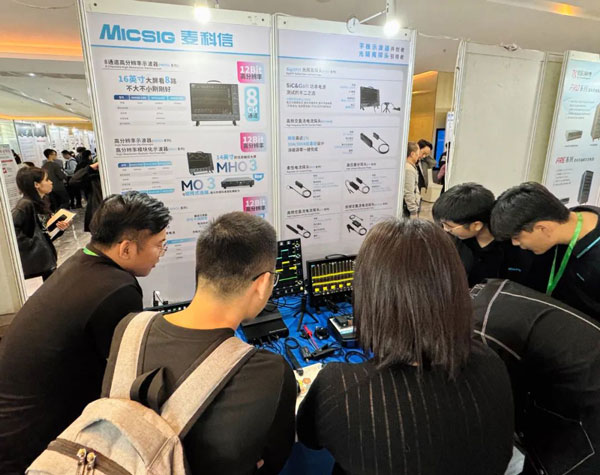
On the day of the forum, the Micsig booth was bustling with activity, with people sharing their practical experiences in power technology. Professional experts "came prepared," bringing test boards to conduct live measurements with optical isolation probes, expressing great satisfaction with the test results.
Micsig has been deeply involved in the industry for many years, as the pioneer of flat-panel oscilloscopes and the leader in optical isolation probes. It has always been committed to addressing the pain points and demands of power industry manufacturers, offering power semiconductor application scenario testing and measurement solutions. This award is a testament to the recognition of Micsig's products by domestic and international industry clients.
Case Study of Optical Isolation Probes

Application of Optical Isolation Probes in Double Pulse Experiments
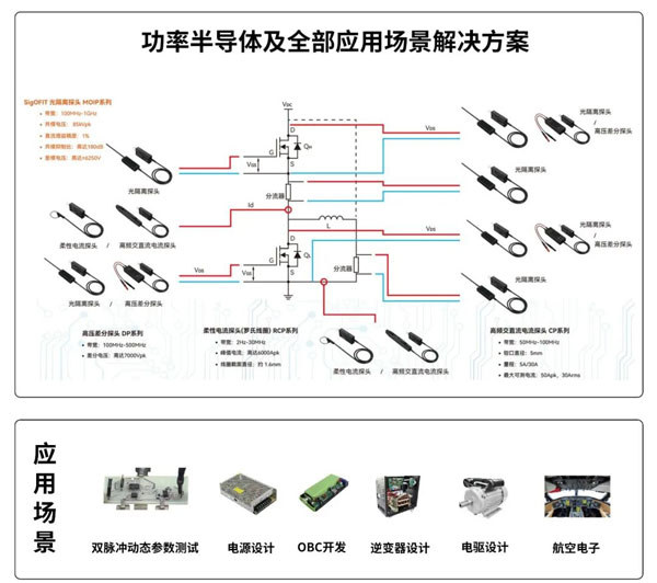
Optical isolation probes play a crucial role in double pulse tests. Taking the half-bridge gate drive circuit of a MOSFET as an example, we need to test the Vds, Id, and Vgs of the lower tube, as well as observe the Vgs of the upper tube. Here, we use optical isolation probes to test the Vgs signal of the upper tube, and also recommend the use of Micsig's MHO high-resolution oscilloscope series 3, with a bandwidth of up to 500MHz, a sampling rate of 3GSa/s, and 4 channels, which can support the simultaneous observation of the switching of the upper and lower tubes, as well as the Id waveform.
Many users may wonder: "We have been using Micsig's DP series high-voltage differential probes, which perform well when testing silicon devices, capable of measuring voltages up to 7000V, with a bandwidth that is not low (500MHz). Now, we have switched to GaN and SiC devices, which should meet the bandwidth requirements for these devices, and can test the lower tube, but why is there always a problem when testing the voltage of the upper tube?"
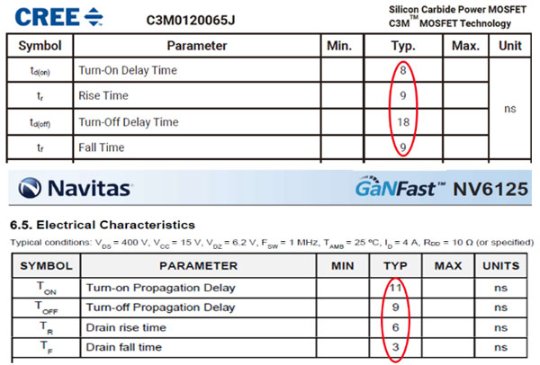
Switching Action Time of Silicon Carbide (SiC) and Gallium Nitride (GaN)
Through data analysis and comparison of the above graph, we found that the switching speeds of silicon carbide (SiC) and gallium nitride (GaN) have reached the ns level. The significant advantage of this feature is that it reduces the energy consumption of the switching power supply, but it also brings huge challenges to the test. In the half-bridge circuit, the Vgs voltage of the upper tube is suspended on the continuously conducting and switching lower tube Vds. The Vds voltage can complete a jump from zero volts to thousands of volts in a few nanoseconds, with high voltage superimposed on high frequency, causing a significant increase in high-order harmonic components. Our measured object Vgs's differential mode voltage is often only a few tens of volts, which will be significantly affected by the common mode interference brought by the high-order harmonic components of Vds. We need to try to suppress this common mode interference when measuring, which requires the test equipment to still have a high common mode rejection capability in the high-frequency band, and this parameter index is called the common mode rejection ratio (CMRR).
Taking Micsig's high-voltage differential probe DP series as an example, at 100kHz, CMRR > -70dB; at 20MHz, CMRR > -40dB; at 120MHz, CMRR is > -26dB. For differential probes, this CMRR is already very excellent in the industry, but it is still far from enough to meet our requirements for measuring the Vgs of the upper tube. We need a test device that still has a high CMRR in the high-frequency band.
Comparison of High-Voltage Differential Probes and Optical Isolation Probes in Actual Measurements
Regarding the impact of CMRR on testing, let's make a comparison to see the problems caused by high-voltage differential probes when testing SiC devices, as well as the comparison of tests with high CMRR probes:
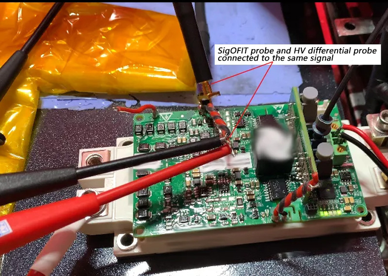
Silicon Carbide IGBT Double Pulse Test, Optical Isolation Probe and Differential Probe Simultaneously Connected to the Upper Bridge Arm Vge Wiring Diagram
Test method: The tested device is an SiC switch with upper and lower tubes, with a Vce voltage of about 500V. High-voltage differential probes and optical isolation probes (using Micsig's optical isolation probe MOIP series) are simultaneously connected to the upper tube Vge signal for double pulse testing.
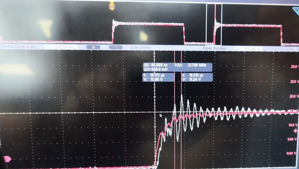
Silicon Carbide IGBT Double Pulse Test, Optical Isolation Probe (Red Waveform) and Differential Probe (White Waveform) Simultaneously Measure the Upper Bridge Arm Vge Waveform Diagram
The above figure is the test result diagram. The white signal in the figure is the test result of the high-voltage differential probe. It can be seen that during the Vge rise, there is a severe up and down oscillation, and the original waveform is almost indistinguishable. We have used high-voltage differential probes to test the Vge signal of the upper tube when the Vce voltage reaches 800V. The oscillation has exceeded the turn-off voltage of SiC, which will seriously affect the judgment of engineers.
The red waveform in the figure is tested using an optical isolation probe, and the signal interference is much less. If the optical isolation probe is tested alone, there is almost no interference. The interference seen here is the impact of the high-voltage differential probe on the optical isolation probe. In fact, the bottom noise of the optical isolation probe is lower than that of the high-voltage differential probe, the accuracy is higher, and the common mode voltage that can be measured is also larger. How is this achieved?
Advantages of Optical Isolation Probes
Micsig uses its exclusive SigOFIT™ technology to select the appropriate attenuator for the size of the measured signal before testing, enabling full-scale testing of differential signals from ±0.01V to ±6250V. While adapting to a wide range of tests, it improves test accuracy (reaching 1%), reduces bottom noise, and increases the signal-to-noise ratio.
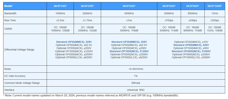
Micsig Optical Isolation Probe MOIP Series Parameter Table
Micsig's MOIP series of optical isolation probes can reach a bandwidth of up to 1GHz, with a minimum bottom noise of less than 0.45mVrms. In the 1GHz band, the CMRR is still above 100dB. Therefore, using optical isolation probes to measure the Vgs of the upper tube no longer needs to consider the impact of common mode interference, perfectly solving the problem of insufficient CMRR of high-voltage differential probes.
In addition, due to the long lead wires (generally about 20cm), the two input wires of the differential probe can be regarded as an antenna, receiving external magnetic field interference. Due to the extremely fast switching speed of gallium nitride, the magnetic field generated by it passing through the input end of the high-voltage differential probe will cause oscillation. Sometimes this oscillation exceeds a certain limit, causing the gallium nitride device to burn out and explode instantly. The optical isolation probe uses MCX or MMCX connections, with extremely short lead wires, almost no antenna effect, and parasitic capacitance within a few pF, eliminating the safety hazards caused by testing.
Summary
Looking to the future, Micsig will continue to uphold the concepts of innovation, professionalism, and excellence, continuously increasing R&D investment to help every electronic field worker and their organizations become more outstanding, contributing tremendous strength to the high-quality takeoff of the domestic testing and measurement industry.
About Micsig
Shenzhen Micsig Technology Co., Ltd. is a leading R&D manufacturer and solution provider of signal testing and measurement equipment in the industry, a national high-tech enterprise, and a specialized, refined, and innovative enterprise. Micsig is committed to the research and development of cutting-edge technologies in the field of signal testing and measurement, especially in the field of oscilloscopes and oscilloscope probes, where we have always been at the forefront of innovation, as the pioneer of flat-panel oscilloscopes and the leader in optical isolation probes.
We adhere to our mission and vision, starting from professionalism, constantly breaking through technological boundaries, helping every electronic field worker and their organizations to be more efficient and outstanding.
Each of our innovations is aimed at breaking through the technological boundaries of products and exploring new possibilities for industry development trends.
The company's main products include oscilloscope series: high-resolution oscilloscopes, flat-panel oscilloscopes, automotive diagnostic oscilloscopes, split oscilloscopes, oscilloscope probe series: optical isolation probes, high-voltage differential probes, flexible current probes (Rogowski coils), high-frequency AC/DC current probes, low-frequency AC/DC current