Common Pitfalls to Avoid Five Vgs Measurement Mistakes
Release Time:2026-09-30
Vgs does not carry the main power, yet it is one of the core signals for judging a power device's switching state, switching behavior, and gate stress. Switching-loss evaluation, dead-time coordination, spurious-turn-on risk, and gate reliability all depend on a trustworthy gate waveform — and to calculate switching loss, Vds and Id must be examined together as well. Wide-bandgap devices such as SiC and GaN have pushed switching events into the nanosecond range; in some applications dv/dt reaches tens or even hundreds of V/ns. In engineering practice, a large share of "device problems measured in the lab" eventually turn out to be "problems of the measurement system". Let's go through the five pitfalls one by one.
Five Pitfalls, One by One
Pitfall 1 | Measuring a floating gate with a single-ended probe
The source of the upper device in a half bridge is not at a fixed potential; it swings between 0 V and the bus voltage with the switching node. Measuring it with a single-ended probe actually captures "gate-to-earth", not the Vgs we want — and if the ground clip touches the switching node, high voltage can be driven straight into the oscilloscope.
Solution: high-side floating Vgs cannot be measured directly with an ordinary grounded single-ended probe. Choose a high-voltage differential probe or an optical isolated probe according to common-mode voltage, dv/dt, and safety requirements, and never connect the ground clip to a high-voltage switching node. The Micsig SigOFIT™ optical isolated probe MOIP series was built exactly for this scenario: isolation is completed at the high-potential side, the front end floats with the measured node within the rated common-mode voltage range, and common-mode voltage reaches up to 85 kVpk. Low-side Vgs is a different story — when the source is close to power ground, a passive or differential probe is fine, and what really deserves attention is the stray inductance of the measurement loop.
Pitfall 2 | Looking only at DC CMRR in high-common-mode scenarios
Datasheet DC CMRR figures of 180 dB look reassuring. But CMRR is specified at a particular frequency and under particular test conditions, and it degrades significantly with frequency — while the energy of common-mode interference is concentrated exactly in the high-frequency band of the switching edge. Taking an 800 V common-mode step with a 5 ns transition as an estimate, the equivalent frequency band is about 70 MHz; if the probe's CMRR has degraded to 60 dB in this band, the residual error works out to roughly 0.8 V — the same order of magnitude as the voltage change near the Miller plateau, turning the waveform into ringing that is impossible to tell real from false.
Solution: select probes by high-frequency CMRR in the equivalent frequency band of the switching edge. Taking 100 MHz — where switching-edge energy concentrates — as an example, the MOIP still delivers 128 dB of CMRR, while many high-voltage differential probes are left with only a few tens of dB in this band; that difference is exactly the dividing line between real and false ringing. Micsig specifies the CMRR at the highest frequency point for every MOIP model: MOIP1200P is 106 dB at 1.2 GHz, MOIP1000P is 108 dB at 1 GHz, MOIP500P is 114 dB at 500 MHz, and all are 180 dB at DC, so you can match the numbers directly to your working conditions.
Pitfall 3 | Ignoring probe input capacitance
Once connected, the probe's input capacitance becomes an extra load in the gate loop, changing the effective gate capacitance, drive bandwidth, and parasitic resonance conditions. When the waveform shows slower edges and reduced overshoot, you need to consider whether it is a circuit improvement or a loading effect introduced by the probe. The gate is a low-energy node, so probe connection inevitably disturbs the circuit.
Solution: choose a probe with low input capacitance as much as possible, and treat "waveform unchanged before and after connection" as the acceptance criterion. MOIP uses a low-input-capacitance design with short test leads and coaxial transmission; with different attenuators the input capacitance can be as low as 1 pF (the exact value depends on the probe model and attenuator configuration).
Pitfall 4 | Picking attenuator and range settings carelessly
If the attenuation ratio is set too high, small signals are compressed too much and the signal-to-noise ratio suffers; if it is set too low, the range is easily exceeded — at best the data is unreliable, at worst the probe is damaged.
Solution: within the measured signal's range, always choose the lowest attenuation ratio available. A single MOIP attenuator covers two ranges — 0 dB and 20 dB switchable at the touch of a button — so even small signals can be captured with high SNR; for even weaker signals, an SMA adapter can be added (±1 V at 0 dB, ±100 mV at 20 dB). If the range is truly exceeded, don't panic — the probe gives an overload indication to remind you to switch ranges.
Pitfall 5 | Treating pin-side waveforms as the true die gate voltage
In non-Kelvin packages, the measured Vgs is actually the voltage between the two external pins of the package. When source parasitic inductance meets high di/dt current, an L·di/dt induced voltage appears — estimated at 3–7 nH and 5–20 A/ns, the theoretical value can reach 15–140 V; the actual value depends on the package, layout, and current waveform. It is not a "false spike": the voltage really exists on the pins, it just does not equal the internal gate-source voltage of the die.
Solution: prefer packages with a Kelvin source; with three-pin packages, distinguish between "pin-side Vgs" and "die-internal Vgs". The Micsig manual also offers a practical method: solder the supplied MMCX or MCX receptacles directly onto the test points with no lead extension as far as possible (when measuring Vgs, connect the receptacle center pin to the gate), minimizing the stray inductance of the measurement loop.
Third-Generation MOIP Optical Isolated Probes: A Powerful Tool for High-Common-Mode Measurement
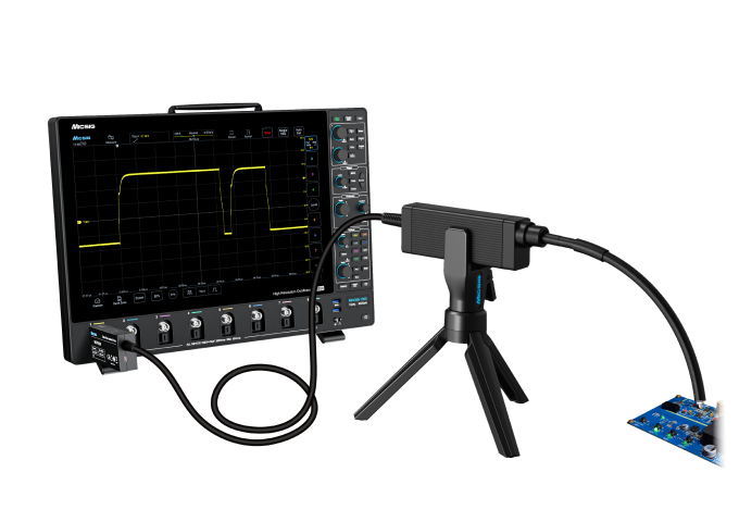
All five pitfalls above come down to the same thing: accurate Vgs measurement relies not on "attaching a probe", but on the probe preserving signal fidelity in a high-common-mode, high-dv/dt environment. That is exactly what the Micsig third-generation SigOFIT™ optical isolated probe MOIP series is designed to do.
The MOIP series takes an "electrical–optical–electrical" approach: the front end converts the electrical signal into an optical signal at the high-potential side, transmits it back over 2 m of fiber (customizable), and the rear end reconstructs it. With no direct electrical connection between front and rear ends, errors from ground loops and common-mode coupling are naturally small. The electrical-optical converter is powered by laser — no battery to install, no extra power cord to run. Combined with Micsig's proprietary ADHOMT analog-digital hybrid laser modulation technology, the probe has zero temperature drift, requires no manual calibration, is ready to use at power-on, and supports 7×24 continuous testing. The probe front end floats with the measured node within the rated common-mode voltage range, making it ideal for high-side floating Vgs and bridge-leg crosstalk scenarios.
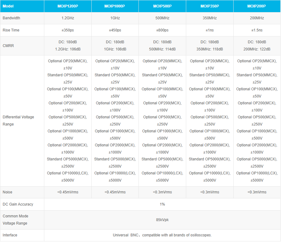
CMRR: 180 dB at DC; MOIP1200P: 106 dB at 1.2 GHz, MOIP1000P: 108 dB at 1 GHz, MOIP500P: 114 dB at 500 MHz, MOIP350P: 118 dB at 350 MHz, MOIP200P: 122 dB at 200 MHz
Common-mode voltage range: up to 85 kVpk
Bandwidth: 200 MHz to 1.2 GHz, in five models — MOIP200P / 350P / 500P / 1000P / 1200P
Differential-mode range: standard attenuators cover ±0.01 V to ±5000 V with full-scale output; higher ranges customizable up to ±20 kV
Input capacitance: as low as 1 pF, with short test leads and coaxial transmission
Accuracy and noise: 1% DC gain accuracy, 1% measurement accuracy within half the bandwidth (gain is flat within half the bandwidth, amplitude error within 1%), noise floor as low as 0.3 mVrms
Daily operation: auto-calibration at power-on in less than 1 second; 0 dB/20 dB range switching; audible and visual alerts for overvoltage and overheating; optional RS-485 converter for remote self-calibration and range switching
Interface and delay: standard BNC interface, compatible with all oscilloscope brands; the 2 m fiber gives a nominal propagation delay of 16.66 ns — simply set the attenuation ratio and delay time in the channel settings per the manual when connecting to the oscilloscope
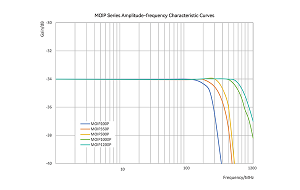
Detailed specifications of each model (captured from the official website specification table):
Companion Platform: MHO Series 12-Bit High-Resolution Oscilloscopes
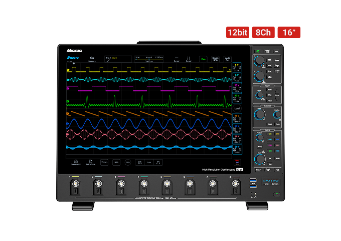
Once the optical isolated probe has extracted the signal, you still need an oscilloscope that can reveal the details. The Micsig MHO68-1000 offers 12-bit vertical resolution, making small details such as the Miller plateau and gate ringing much easier to see; with 1 GHz bandwidth, 6 GSa/s sampling, and 180 Mpts deep memory, it handles both nanosecond switching edges and long time windows; with 8 channels acquiring in parallel, the Vgs / Vds of the upper or lower device plus Id can be viewed simultaneously — no separate measurements, and no worry about mismatched operating conditions between runs.
From probe to oscilloscope, Micsig provides a complete solution for Vgs measurement.
Note: product parameters in this article come from publicly available material on the Micsig official website; please refer to the latest datasheets for specifics.